“Our solution expertise is based on a deep understanding of processes”


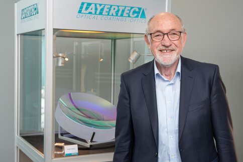
As a supplier of precision optics with a large number of modern in-house coating systems – including systems for magnetron and ion beam sputtering, thermal and ion-assisted electron beam evaporation – LAYERTEC has developed into a leading global optics manufacturer with 400 employees since its foundation in 1990. Founder Dr. h.c. Hartmut Heyer, who remains a member of the company’s management team, provides in-depth insights and outlooks on the technological and economic development of the market for high-performance optical components and coatings in a PHOTONICS interview.
Congratulations on your honorary doctorate! Like the Ernst Abbe Prize in 2022, this award is dedicated to your entrepreneurial and scientific work. What does it mean to you?
Dr. Hartmut Heyer: A doctorate was never a priority for me. To me, it’s actually always been more important to get on with the job itself. I got involved in practical technology development at the Institute of Physics at the University of Jena at an early stage and soon had a solid base of customers from universities and industry who ordered laser optics from us. I received a lot of recognition from them. The honorary doctorate is a special recognition of my work and is therefore very important to me.
Your contributions to magnetron sputtering technology for coating laser optics are considered groundbreaking – and were the basis for the continued success of LAYERTEC GmbH, which you founded in 1990. Can you take us back to the beginnings, shortly after the German reunification?
Heyer: There was practically no entrepreneurial middle class in the GDR. In Jena, there was ZEISS, a large company with rather rigid structures. Special laser and optical solutions were hard to come by. The universities therefore set up pilot plants in which they developed such solutions themselves and also produced them on a small scale for industry. I was already a research engineer for the production of optical coatings in Jena in the 1980s and specialized in sputtering technology. I quickly gained customers – including ZEISS. Magnetron sputtering was brand new at the time. Unlike established evaporation processes, it is based on a plasma process: Heavy noble gas ions from the plasma are accelerated to a cathode – known as a sputtering target – from which they knock out metal atoms on impact. These then form the actual layer. For transparent layers, oxygen is added, with which the metal atoms react during layer formation on the substrate surface and form oxide layers. Sputtering gained its practical significance with the introduction of magnetron sputtering sources. The additional magnetic field significantly increased the plasma discharge, which enabled higher coating rates and made sputtering practical – and economical – for transparent optical coatings in the first place.
How was it that you got into this technology so early in the GDR?
Heyer: We were among the pioneers. In 1983, we received the first magnetron sputter source from the Manfred von Ardenne Institute, which corresponded to the international state of development. We converted an existing sputtering system and started to produce and optimize single layers. The system had four sputter sources, which over time enabled us to produce the first multilayer systems based on various single layers. In 1984, for example, we produced the first helium-neon laser mirrors, which immediately had a reflection of 99.96 percent. This was an excellent value compared to vaporized mirrors. With these sputtered optical multilayer systems, we quickly attracted the attention of leading research institutes – including the laser laboratory at the University of Jena, the Physikalisch-Technisches Institut Jena and the Zentralinstitut für wissenschaftlichen Gerätebau in Berlin.
How did the company come to be founded?
Heyer: Before the fall of the Berlin Wall, we had already joked that we would actually have to spin off with the technology – but that was politically impossible. But something remained: Our sputtered coating systems were very stable against environmental influences, had minimal optical losses – and there was demand. With the fall of the Berlin Wall in 1989, I immediately began to push ahead with the spin-off. The institute supported me in this. I was able to take over the sputtering system and laboratory equipment. We got started together with a doctoral student and a gifted technician who knew the system inside out: The first promotional projects, the first contacts with LASEROPTIK in Hanover, who introduced us to many customers for whose requirements our sputtering technology was suitable. This gave us our first valuable industry contacts. One project involved tracking the exact laser power for stable process control during laser welding. As a measure of the laser power, a detector behind the highly reflective resonator mirror should measure the light still passing through. It turned out that this could only be done with our environmentally stable, sputtered coatings. This showed us that we could keep pace technologically in Western markets. That was very encouraging for us. Incidentally, this project led us indirectly to TRUMPF, with whom we have also had a good relationship ever since.
How have coating technologies developed since then?
Heyer: When we started, sputter-based coating processes were still in their infancy. Today, they are ubiquitous – and an important alternative to vaporization technology. Both have their strengths: Layer formation is a complex process influenced by chemical and physical factors. Stoichiometry and structure of the oxide layers depend on the kinetic energy and the excitation states of the layer-forming particles in the plasma. Smooth, structureless layers are important in high-end applications, as coarser structures cause light to scatter. The sputtered stoichiometric, very dense oxide layers, on the other hand, minimize absorption and scattering losses. In contrast to thermal evaporation, these parameters can be better controlled in the plasma process, which opens up possibilities for layer optimization. We have become better and better at this over the years.
In which fields of application are coating technologies particularly suit-able?
Heyer: In particular, the rapid development of laser technology has always placed new demands on coatings. The mirrors must not become hot even at the highest CW power levels and constantly increasing pulse power densities must not destroy the mirrors. Laser-optical devices and measuring systems are becoming increasingly precise and complex, which places ever greater demands on the spectral accuracy and stability of the components. In general, the aerospace and defense sectors also drove advances in coating technology. For example, laser gyroscopes, which are used to navigate rockets, require mirrors with the lowest losses and highest reflections. Ion beam sputtering was developed in the USA for this purpose. Another important driver was the triumphant advance of optical data transmission in the telecommunications sector, which has set standards in terms of accuracy and stability for filters: for example, highly stable, nanometer-precise optical wavelength filters for delimiting optical channels.
What are the biggest challenges for optical coatings?
Heyer: It’s difficult to put your finger on it. You will always find suppliers who can realize over 99.999 percent reflection or particularly smooth, low-scatter substrates or particularly dense layers. However, in many applications it is important to find the optimum compromise in order to be able to meet conflicting requirements for a highly specific, customized component. To this end, it is good to have a wide range of expertise in-house - in addition to coating, we also have our own optics production and production-related areas such as metrology, design, mechanics, electrics and electronics. This gives us the necessary process understanding to develop solutions for highly specific requirements. In some cases, it is a question of flatness in the nanometer range and compliance with parameters that contradict each other. They can only survive in today’s high-tech markets when the overall package of reflection, flatness, density, cleanliness, damage resistance and minimized absorption in the ppm range is right. Added to this is the increasing variety of pulse durations, the variety of shapes of the optics and the increasingly broad spectrum of wavelengths in laser processes from extreme ultraviolet to deep into the infrared range. All of this constantly poses new challenges for us and our research and development. At the same time, that’s what gives it that extra something for us! This makes our experience and expertise increasingly important.
What role have metrological innovations played in the progress of optical coatings?
Heyer: Electronics and measurement technology have undergone a revolution since the 1990s. What we implement today with measurement and control technology was unthinkable back then. Optical monitoring has made vaporization technology more and more precise. In sputtering, we are now able to prevent breakdowns during operation: Oxide layers form not only on the substrates, but also on the target surface from which we remove the metal atoms. Charge carriers that accumulate there can generate voltage differences that discharge spontaneously. To prevent these flashovers, the process is interrupted for microseconds so that the electrons in the plasma defuse the accumulated layer of positive charge carriers. Thanks to modern semiconductor and measurement technology, this can be detected and controlled with such precision that we can even prevent voltage discharges from starting. The networking of coating systems and the integration of sensor technology for tracking process parameters have been extremely helpful in bringing sputtering and vapor deposition processes up to today’s standards.
LAYERTEC is renowned in terms of technology. How does a medium-sized company with 400 employees manage to maintain its leading position at an international scale?
Heyer: The key – and measurement technology also plays a central role here – is reproducible quality. If we offer coatings with less than one part per million (1 ppm) absorption, we have to be able to measure this. To do this, we have a cavity ring down (CRD) device that measures the lifetime of the light in the resonator and the reflection from its mirrors. We have extended the process in-house from a single wavelength to a range of wavelengths. This is how we have often proceeded. If a technology is good but does not fully meet our specific requirements, we develop it further ourselves. This is where our deep understanding of the process comes from. We want to understand why a process is running differently than we had imagined – and how we can change this. And measurement technology is the key to this. We always want to do things as well as possible and solve problems for our customers that other providers struggle with. The real challenge is being able to reproduce such solutions in large quantities at any time. So far, we have almost always managed to master them.
Global competition is also constantly increasing in your market segment. Can the continued growth of photonics compensate for the increase in competitors?
Heyer: Of course, there are also very good providers in other regions of the world – be it China or the Baltic states. We sense that competition is increasing. But the market for optical coatings is very broad. We operate in market segments in which we have to – and are able to – meet the highest demands of our customers. We are not the cheapest. But what we deliver generally works reliably right from the start. Customers keep telling us that it is often ultimately more expensive to use cheaper but less reliable optics due to the higher integration costs. In the end, increasing competition primarily affects providers whose products and expertise are interchangeable. We have a different aim. Thanks to our in-depth understanding of the process, we can offer our customers not only all conceivable optics with the right coatings for them – but also solution expertise. And this will become more and more important in the future in light of the increasingly broad and specific use of photonics.