Metasurfaces as lens and mirror substitutes


The Fraunhofer Institute for Applied Optics and Precision Engineering IOF in Jena demonstrated a microstructured metasurface with a diameter of three decimeters at LASER. The technology has disruptive potential.
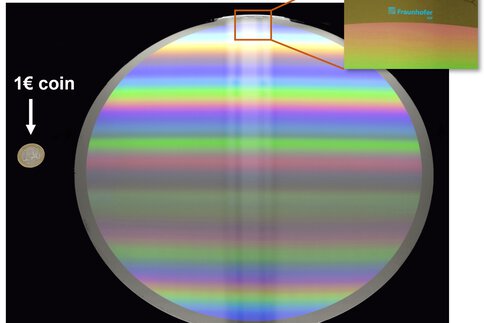
“Bye bye, lens. Hello metasurface!” This is how Fraunhofer IOF introduces its press release on a manufacturing breakthrough, the product of which was on display at LASER World of PHOTONICS 2023 in June: a metasurface of nearly 30 centimeters (cm) in diameter, which the research team structured over its entire surface, using electron beam lithography with customized resonators on a nanometer scale. Due to the very time-consuming nanostructuring process, metasurfaces have rarely been larger than a few square millimeters.
The new process could make metasurfaces interesting for industrial applications. For example, as a flat, space-saving alternative to bulky lenses and mirrors. While these can only fulfill their optical function—such as focusing, directing or scattering light—thanks to their macroscopic geometry, the optical function of the metasurfaces can be defined in each case on an application-specific basis through the design of their nanostructures. For this reason, they are often superior to conventional optics, not only in terms of installation space, but also in terms of their optical function. Adaptive wavelength-dependent diffraction is made possible thanks to the light-structure interaction, which can be defined by design. Specific absorption properties, polarization-dependent behavior of the metasurfaces, and nonlinear optical responses that can be used for wavelength conversion can also be inscribed in the metasurfaces under computer control.
Precision of electron-beam lithography becomes usable on a large scale
The IOF team led by Professor Uwe Zeitner from the Scientific Directorate and Dr. Falk Eilenberger, head of the Department of Micro- and Nanostructured Optics, has been researching manufacturing strategies to make electron beam lithography usable on a larger scale for many years. In a paper published in the Journal of Micro/Nanopatterning, Materials, and Metrology they report just how much the devil is in the detail. In principle, the team is looking for ways to shorten the very time-consuming lithographic structuring process—and to minimize any interfering influences on the subsequent light-structure interaction.
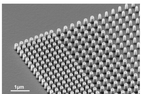
For patterning, the IOF team first applies a chromium-based and a photosensitive functional layer to a silicon wafer. After exposure, the unexposed portion of the photosensitive layer can be ablated. The resulting nanometer-precise pattern can then be transferred to the chromium layer by dry etching. This lays the foundation for further processing: after the residual photosensitive layer is removed, the structured chromium layer serves as a template—or hardmask—for an ion etching process that transfers the high-precision structure to the wafer surface. Once the remaining chromium mask has also been removed, the silicon structure can be used as an optical element—or as a master for replications.
New exposure strategy is up to ten thousand times faster
If the nanostructures on a 30-cm metasurface were exposed point by point at the beginning of the described process chain, this would take weeks or even months, depending on the complexity of the structure. With a view to industrial applications, much more efficient exposure strategies are required. Approaches for this are variable shaped beam (VSB) exposure with which structures based on rectangles or triangles are exposed block by block. Up to four square micrometers (µm2) can be exposed per light pulse, provided that the individual blocks can be positioned with nanometer precision. After all, we are talking about structures on a nanometer scale, which have to be introduced into the substrate with nanometer-precise gaps between each other. An additional difficulty is that, when inserting the pattern blocks (similar to the joints in brickwork), there is a risk of macroscopic superstructures forming. Because these deflect incident light, researchers refer to them as “diffraction ghosts”.
In the technical paper, the team explains how they succeeded in preventing the periodic occurrence of these diffraction ghosts by a special shaping of the stencil in the so-called Character-Projection-(CP)-exposure process. Ultimately, this allowed them to fabricate the world-record scale metasurface via electron beam lithography without ghostly superstructures. At the same time, the new manufacturing process achieves the necessary nanometer-scale patterning resolution as well as the required positioning accuracy and pattern fidelity. Because exposure with their CP strategy is also several orders of magnitude faster than point beam exposure, the IOF researchers believe that key requirements for industrial use of metasurfaces have been met. “With our character projection, very high-resolution structures can be exposed in parallel at high speed,” Zeitner explains. The process is thus poised to produce nano-optical structures up to element sizes of several hundred square centimeters.
Disruptive potential for a wide range of applications
In the paper, the team lists a broad spectrum of potential applications, ranging from gratings for ultrashort laser pulses to high-resolution spectrometers and computer-generated holograms for aspheric testing to optical meta-lenses and UV polarizers with locally different orientations. The disruptive potential of metasurfaces is also based on the fact that they make it possible to build optical systems significantly thinner. “This technology can revolutionize optical imaging systems,” explains Eilenberger, as it combines smaller installation space requirements with increased optical functionality. Nano-optical metasurfaces are likely to show their strengths wherever large deflection angles are required in a small space, such as in virtual, mixed and augmented reality glasses, in smartphones or in miniaturized high-resolution spectroscopes.