Precision Analytics in the Nano Cosmos
In addition to structural measurements on nanometer and picometer scales, optical material analyses and vibration measurements in the nanocosmos are also becoming more widespread.
“With our solutions for nanopositioning, laser interferometry, imaging, and spectroscopy, we enable morphological as well as substantial analyses of surfaces in molecular resolution,” says Peter Kraemer, CEO of attocube systems AG. Interface and surface research teams use the solutions but they are also found in the areas of (nano)plasmonics and graphene research. In other words, promising future fields that open up a new chapter in materials research, since researchers are not only able to look deeper into molecular and atomic structures, but can also analyze and measure them at the same time. The nanoanalytics platforms are based on the company’s own laser technology developed in collaboration with partner companies. Surprisingly, attocube uses normal wavelengths of FTIR (Fourier transform infrared) spectroscopy in the range between 2 and 15 µm. That raises the question as to how nanostructures that are so much smaller can be captured with these long waves. The answer lies in a trick that experts know as scattering scanning near-field optical microscopy. Kraemer explains it like this, “We direct the laser at an extremely sharp, light-scattering tip, which generates a nano-scale near-field focus. This uncouples the resolution from the wavelength that is used.” This tip also detects the spectra emitted from the sample. The crux of the matter is the separation of signals from introduced and reflected light. attocube is a leader in this area.
With the nano-FTIR process, it is possible to investigate individual nano-structures with visible infrared light and even in the terahertz spectral band. And since no aggressive short-wave UV radiation is used, highly sensitive, non-destructive, chemical analyses are possible in the low double-digit nanometer length range. “It is particularly smart that the materials can be clearly identified based on their spectral signatures from the field of conventional IR spectroscopy,” explains Kraemer. That is the key for multimodal analysis, which, among other things, makes time-resolved pump sample spectroscopy accessible for users in nano-research.
However, attocube will have different focuses at LASER World of PHOTONICS 2022. One of these is quantum technology, where the roots of the company are. Because there were no nanopositioners available for cryogenic environments to fix quantum dots, the company’s founder, Professor Khaled Karraï, developed them himself. And because nanopositioning is possible only in combination with high-precision measuring technology, this was followed by more patents for 3-axis interferometers based on fiber-coupled diode lasers. They were able to capture signal changes with pm-level accuracy and, thanks to the fiber-based measurements, were extremely robust with regard to environmental influences. For LASER, Kraemer has announced various new products in the field of low-temperature-capable components and optical cryostats. These include a very compact cooling system with mobile compressor. “It removes the dependence on complicated laboratory infrastructure and paves the way for quantum technology applications in the industrial environment,” he tells us.
Future Solutions for Vibration Analysis
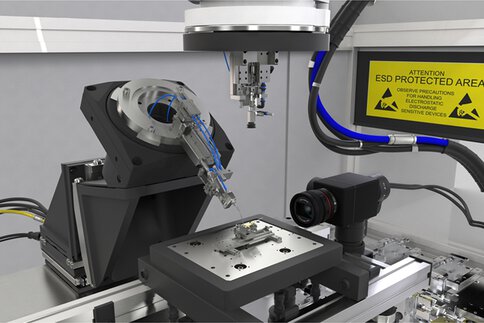
While attocube enables multimodal materials analysis, SmarAct and SIOS Meßtechnik GmbH are pushing ahead with vibration analyses in the nanocosmos. SmarAct offers the “PicoScale Vibrometer” with measurement bandwidths to 2.5 MHz and <1 picometer (pm) resolution. This can be used to investigate vibration modes of tiny components. According to Semjon Köhnke from the company’s technical sales department, the measurements use interferometry-based position detection with a frequency of 2.5 MHz, which detects even the tiniest change in position. The laser vibrometer scans the surface of the sample to make the vibration modes visible. For MEMS (microelectricmechanical systems) manufacturers, the process is important to check the functions of miniaturized microphones, speakers, ultrasonic transducers, or acceleration and rotation sensors. To detect very low frequencies, instead of conventional Doppler vibrometry, the Michelson principle, which records position changes over time, is used. The process also delivers topographical images of the measured object. The combination of an NIR laser with confocal optics even allows the inner structures of encapsulated MEMS to be investigated through their silicon layers that are semi-permeable for NIR wavelengths.
SIOS also offers solutions for laser-interferometric vibrometry with resolutions well into the picometer range. Areas of application: research labs, particle accelerators, and synchrotrons. “While research projects are often subject to secrecy, the picture in the industrial area is clearer,” explains Sales Manager Peter Grundschok. Here, customers use the ultra-precise analysis to optimize the vibration behavior of machinery components, in the haptic design of touchscreens and other functional surfaces, and to design micromembranes in hearing aids, in-ear speakers and mobile devices. At LASER from April 26 to 29, SIOS will not exhibit its entire range of length and vibration measuring equipment, but they will be presenting a few new products. “These include a very compact, frequency-stabilized helium-neon (HeNe) laser, which contributes to the miniaturization trend in measuring equipment,” he reports.