The Miniaturizers
Whether it’s high-precision optics, miniaturized pacemakers, hearing aids, microphones or speakers or material analyses on a molecular scale—the enablers use light to make micro, nano, and even picometer structures measurable.
The miniaturized world is full of wonders. With EUV lithography, chip manufacturers are able to put 10 billion transistors on an area the size of a fingernail. In the process, mirrors are used whose maximum geometrical deviation calculated over an area the size of Germany is just 0.1 mm. Research laboratories analyze surfaces in molecular resolutions. And in particle acceleration, tiny vibrations that occur when particles collide with sensors can be measured. Thanks to ultra-precise vibration measurement, minute microphones and speakers in smartphones, in-ear speakers and hearing aids ensure the purest of sounds. MEMS (microelectricmechanical systems) are becoming increasingly popular as sensors and actuators as well as acoustic and optical components in all areas of our modern world.
To implement all of these wonders on a microscale, there is a key requirement. “You can only produce and optimize something that can be measured,” said Professor Wolfgang Osten in a PHOTONICS interview in 2017. These days, measurement technology is edging forward into the realms of the unimaginable for human beings. It measures mirrors and any shape of lens without which space exploration and chip structures in the single-digit nanometer range would be unconceivable, checks wafers and MEMS in production for faults, positions test objects in atomic force microscopes and calibrates machinery for high-precision processes. And all of that with resolutions in the nano and picometer range. Exactly what does that mean?—If you could line up one billion same-sized beads on one millimeter of string, each of these would be one picometer (pm). If you could only fit one million beads onto the millimeter of string, each of them would be one nanometer (nm)—still much too small for the human eye and motor functions. But, still, these dimensions can be measured reliably. Scientists in synchrotrons and an increasing number of laboratories are also using this technology, as well as manufacturers of chips, MEMS, precision optics and sensors and the pioneers in quantum engineering. Their most important measuring tool is light.
Interplay between Nanopositioning and Interferometry
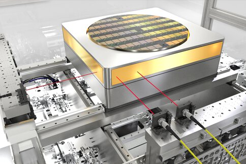
Because resolutions in the sub-nanometer range are well below the classic resolution limit (Rayleigh criterion)—laser wavelengths used in optical measurement processes are often in the infrared range from 800 nm—manufacturers of measurement equipment have to dig deep in their bag of tricks. This begins with nanopositioning over sections that are, in some cases, centimeters long. The piezo drives required for this can be obtained from about a dozen LASER exhibitors, including attocube, nanoFaktur, Physik Instrumente (PI) and SmarAct. In linear slip-stick drive systems and small rotation stages, piezo elements that expand minimally under voltage ensure (sub)-nanometer feed rates. “Over the last two decades, we have continuously developed this drive technology in many different areas of application so that we are now able to offer specific solutions for very low temperatures, ultra-high vacuum environments, and strong magnetic fields,” explains attocube CEO Peter Kraemer. This nanopositioning technology is now used in extremely challenging environments, such as wafer inspection systems, particle accelerators, special microscopes—and, increasingly, also in quantum computers.
Interferometry-based measuring systems and positioning technology work hand in hand. “Measuring technology is often used as a tool for precise position determination,” says SmarAct expert Semjon Köhnke. “We integrate it in our positioning systems to control movement down to the sub-nanometer range. Our customers then have a turnkey solution where all they have to do is pass on the desired position to the control unit. The position, measured by interferometer, is stored in a controller which readjusts to the respective desired position.” This is used mainly by high-tech companies and elite researchers who are pushing the boundaries of what is technically feasible with SmarAct solutions: this includes precise real-time control with consideration of vibration and temperature-related drifts in synchrotron experiments, integrated measurement and positioning in cryogenic environments of quantum computing as well as precise wafer inspection in the sub-nm range. For this, the interferometers achieve signal resolutions to 1 pm. The heart is a compact Michelson interferometer that measures the difference between two laser beam paths. For that purpose, the reference beam is fixed at almost zero by coating one side of the beam splitter with a highly reflective surface. The measuring beam passes through the other, anti-reflection coated side of the beam splitter. Since in the picometer range, even the influence of temperature and pressure fluctuations counts towards the refraction index of the air, SmarAct captures these interferences with sensors in order to computationally eliminate them from the measured values. Alternatively, both partial beams can be directed towards the measured object where the reference beam measures a fixed position basis. “Since the interferences have an equal effect on both beams, they balance each other out,” explains Köhnke.
Guaranteed Precision with Interferometry
In the nano and pico worlds, it is essential that environmental influences are eliminated. That’s why SIOS Meßtechnik supplies laser interferometry precision measuring equipment for calibration and nanomeasurement technology, including solid acoustic hoods, in order to encapsulate the measurement of interfering influences, according to Sales Manager Peter Grundschok. In addition, temperature-stable materials such as the glass-ceramic Zerodur and the metal Invar are used. They minimize expansion-related drifts even when measuring in air-conditioned compartments. Calibrated environmental sensors and interferometers, which record differentially all positions of the measuring table in x, y and z directions, are used for additional protection. In order to permanently ensure optimal operation of these nano-measuring machines, customers—which include various national measurement institutes, including the PTB—are given user trainings and intensive advice when selecting and preparing the site.
“The trend in measuring technology is moving towards higher measurement resolutions with increasingly smaller positioning steps coupled with faster delivery movements,” explains Grundschok. The company offers wafer and chip producers the permanent integration of differential interferometers into their systems. Other customers used the adapted measurement technology to calibrate coordinate measurement machines or machine tools for high-precision processes, where easy, reliable handling and fast commissioning were required. Cantilevers in atomic force microscopes are also calibrated using nanomeasurement technology by SIOS. So, the circle is complete: with atomic force microscopy (AFM), the ultra-precise EUV mirrors that enable chip structures in the single-digit nanometer range are tested for their dimensional accuracy. AFM microscopy calibrated with laser-interferometer-based vibrometry provides nm-precise images of the surface on a molecular level.
While everyday technology is moving toward the nanostructure range, the metrology miniaturization enablers have long been active in pico worlds. They are also making advances in the robustness of their measurement technology. AMETEK Zygo offers vibration-resistant interferometry under non-controlled environmental conditions. Account Manager Torsten Glaschke explains what is behind this: “On the one hand, fully dynamic measurements are based on the familiar carrier-fringe process. In this process, a static multiple-stripe pattern is evaluated with Fourier analysis within a few microseconds. With adequate averaging it is possible to eliminate interference from vibrations and turbulence that each single one of the recorded stripe patterns contains.” With less intense vibrations, the vibration-resistant evaluation algorithm “QPSI”, developed by Zygos, comes in to play. This model-based phase-shifting measurement eliminates measurement artifacts that occur even with mild to moderate vibration. Will laser interferometry soon be used in production processes? Glaschke sees the benefits more likely in higher measuring accuracies, clearer comprehensibility, increased reliability and less effort in the measurement processes. Success is just around the corner. The miniaturization enablers are experiencing strong demand for high-precision measurement technology especially from the semiconductor industry.