

Electronics and Photonics in Productive Symbiosis

With the world’s leading trade fairs—electronica in November 2026 and Laser World of Photonics in June 2027—Messe München is bringing together two of the industry communities with the greatest impact of all. Working in close symbiosis, they are currently accelerating their pace.
CMOS technology demonstrates the enormous technological impact that arises when electronics and photonics work together. At the same time, it is one of the most important drivers of progress within these two technological fields themselves. It is an effect reminiscent of cell division, except that here we are dealing with exponential progress. But first things first.
Traditional CMOS (Complementary Metal Oxide Semiconductor) technology is central to the performance enhancement and ongoing miniaturization of processors (CPUs) and graphics processing units (GPUs), as well as transistors for power electronics—all of which are built on silicon wafers and in which electrons serve as the medium for signal transmission. Simply said, it is based on nanometer-scale on/off switches, of which more than 100 billion are now packed onto microchips the size of a fingernail.
This enormous packing density is pushing classic CMOS electronics to its limits. Electrical resistance and the resulting latencies and heat, as well as their electromagnetic sensitivity, call for new approaches. Photonics provides them. CMOS 2.0 solutions complement the logic of classical CMOS electronics with electro-optics, enabling data transmission at the speed of light between computing cores, in data centers, or in increasingly networked manufacturing environments. Furthermore, signal transmission using photons is unaffected by either electrical resistance or electromagnetic interference. At the same time, it minimizes heat generation—and thus energy losses. This literally “integrated” photonics comes at just the right time for the global boom in energy-hungry AI data centers.
Key Technology for Smartphones, Digital Cameras, and Industrial Image Processing
Photonics and optical components integrated directly on chips convert electrons into photons and vice versa, transmitting data at the speed of light. These components rely on the same physical effects as LEDs, photodiodes, and diode lasers, which are based on the conversion of light into electrical signals and vice versa. CMOS sensors are also the key to increasingly powerful, high-resolution image sensors for digital cameras, smartphones, microscopes, and industrial imaging.
These enable increasingly powerful inline quality inspections in electronics and semiconductor manufacturing, as well as increasingly precise laser processes monitored by optical sensors. In semiconductor and electronics manufacturing, highly efficient diode lasers in the appropriate wavelengths—ranging from ultra-short-wavelength ultraviolet to long-wavelength infrared—are being used increasingly. As LASER exhibitor Laserline states: “Whereas initially components at the end of the production line were marked and labeled with lasers, today the scope encompasses many more manufacturing steps—from thermal applications at the start of wafer production (rapid thermal annealing) to remelting processes, for example using blue diode lasers (crystallization/dopant activation) to targeted illumination for defect detection in intermediate products. Depending on the application, a wide variety of pulsed and cw-lasers are used across a very broad range of power levels and wavelengths.”
The synergy between electronics and photonics in semiconductor lasers thus paves the way for increasingly productive, high-quality, and cost-efficient processes in the also increasingly miniaturized semiconductor and electronics manufacturing. It is a cascade of progress that accelerates exponentially, much like cell division—and at the same time gives rise to an ever-greater variety of functionalities. To this end, photonics complements electronics—with its logic control circuits—through integrated active optical components, including not only lasers but also modulators, detectors, optical fibers, as well as optical fibers and their connectors.
The Challenge of Packaging
A prerequisite for this is extremely precise packaging. And here, electronics and photonics provide their own solutions either—ranging from nanometer-precise positioning systems and ultra-precise measurement, control, and regulation technology, which various vendors are showcasing at both LASER and electronica—to sub-micrometer-precise alignment of optical fibers and light sources, which is among the core competencies of various LASER exhibitors and the automation specialists exhibiting concurrently at automatica. However, advances in packaging begin as early as the chip design stage—and here, too, the interplay between electronics and photonics is now opening up new possibilities. To achieve even greater chip performance in even less space, the semiconductor industry has recently turned to glass substrates, into which it uses lasers to create millions of microscopic holes that are then coated with conductive material. LASER exhibitor TRUMPF provides the photonic solution for precise perforation with its HiPIMS process. This makes it possible to reliably create very deep and narrow holes in the glass to produce flawlessly coated through-silicon vias.
TRUMPF’s HIPIMS generators produce a highly ionized plasma. The ions can be precisely controlled using electric and magnetic fields and directed into deep, narrow holes. Ionization ensures a higher density of the molecules introduced during coating—thereby creating the conditions for extremely homogeneous coatings. According to TRUMPF, these coatings are the key to higher manufacturing yields and, consequently, to cost-effective mass production of future high-performance AI-Chips. But this is by no means the only photonic contribution to more powerful microchips. For example, ultrashort pulse lasers are used to drill the deep, narrow through-glass vias into the glass substrates. And TRUMPF, together with ZEISS and the Fraunhofer IOF, is also the originator of the laser-based EUV lithography that enables structure sizes as small as 4 nanometers on wafers.
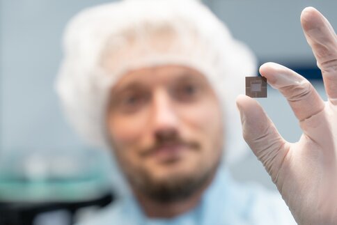
Photonics—the backbone of ever-more-powerful electronics
But even nanometer-scale structures are not the end of the line. Chip manufacturers are currently moving toward stacking and connecting chips to enable even more computing power in even less space. This requires new heat dissipation solutions to prevent the chip stacks from overheating. The solution lies in microfluidic channels, which must be incorporated with high precision into structures made of extremely hard silicon carbide. Here, too, the method of choice comes from photonics: ultrashort-pulse lasers can not only drill the channels into the stacks five times faster than conventional etching processes but also ensure very smooth surfaces in the cooling structures, which are precise to the micrometer. Photonics is thus paving the way here as well for higher quality, energy efficiency, and cost efficiency in electronics.
These and many other examples show that it can be worth the effort for LASER exhibitors to showcase their expertise at the electronica, too—and vice versa. Because all in all, progress is emerging from the close symbiosis of electronics and photonics.